BENDIX BENDIX 7129 Uživatelský manuál Strana 1
Procházejte online nebo si stáhněte Uživatelský manuál pro Pračky BENDIX BENDIX 7129. ADV7129 192-Bit, 360 MHz True-Color Video [en] Uživatelská příručka
- Strana / 20
- Tabulka s obsahem
- KNIHY

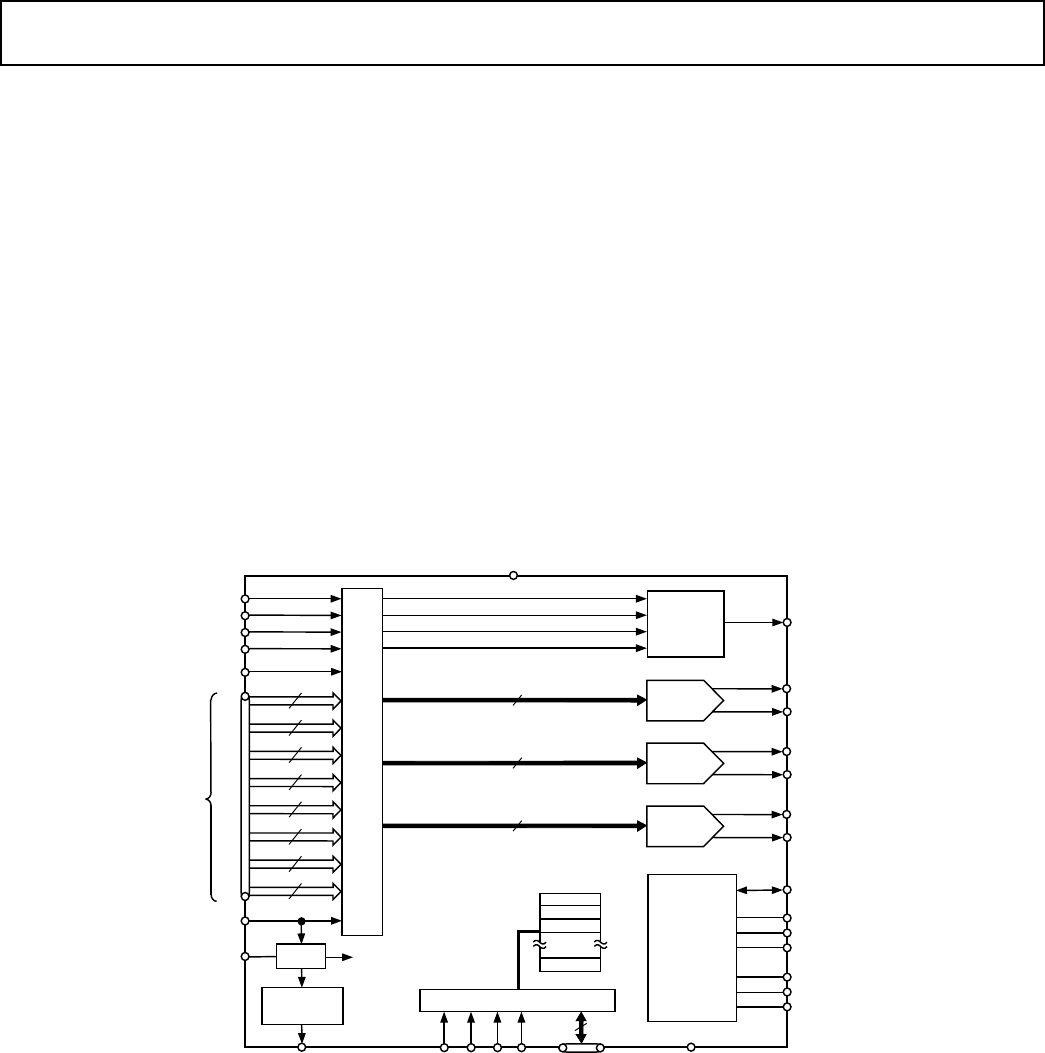
- 192-Bit, 360 MHz True-Color 1
- Video DAC with Onboard PLL 1
- ADV7129–SPECIFICATIONS 2
- TIMING SPECIFICATIONS 3
- DIGITAL INPUT TO ANALOG 4
- OUTPUT PIPELINE 4
- WARNING! 5
- PIN ASSIGNMENTS 6
- *No Connect 7
- Figure 5 8
- Figure 6. Control Registers 11
- Figure 7. Command Register 1 11
- Figure 8. Command Register 2 12
- Figure 9. Gain Error Register 12
- AND VIDEO OUTPUTS 13
- Thermal Model 17
- APPENDIX II 17
- Package Characteristics 17
- OUTLINE DIMENSIONS 18
- PRINTED IN U.S.A 20
- C2215–6–10/96 20
Shrnutí obsahu
REV. 0Information furnished by Analog Devices is believed to be accurate andreliable. However, no responsibility is assumed by Analog Devices for itsu
ADV7129–10–REV. 0SENSEIf any one or more of the analog outputs, IOG, IOR and IOB,exceed the internal voltage reference level (due to absence ofCRT), S
ADV7129–11–REV. 0REGISTER PROGRAMMINGThe following section describes each register, including AddressRegister and each of the Control Registers in ter
ADV7129–12–REV. 0COMMAND REGISTER 2 (CR2)(Address Register (A10–A0) = 411H)This register contains a number of control bits as shown in thediagram. CR
ADV7129–13–REV. 0DIGITAL-TO-ANALOG CONVERTERS (DACS)AND VIDEO OUTPUTSThe ADV7129 contains three high speed video DACs. TheDAC outputs are represented
ADV7129–14–REV. 0Table I. Video Output Truth Table (RSET = 398V, RLOAD = 37.5V)O/P with Sync O/P with Sync DACDescription Enabled (mA) Disabled (mA) S
ADV7129–15–REV. 0APPENDIX IBOARD DESIGN AND LAYOUT CONSIDERATIONSThe ADV7129 is a highly integrated circuit containing bothprecision analog and high s
ADV7129–16–REV. 0PIXELDATA192RBIASGBIASBBIASRCOMPGCOMPBCOMPIORIORIOGIOGIOBIOBRRSETGRSETBRSET+5V(VAA)ANALOG POWER PLANE10µF33µFFERRITE BEAD+5V(BOARD SU
ADV7129–17–REV. 0APPENDIX IITHERMAL AND ENVIRONMENTAL CONSIDERATIONSThe ADV7129 is a very highly integrated monolithic silicondevice. This high level
ADV7129–18–REV. 0OUTLINE DIMENSIONSDimensions shown in inches and (mm).304-Lead Plastic Quad Flatpack(S-304)SEATINGPLANE0.167 (4.23)NOM0.150 (3.80) NO
ADV7129–SPECIFICATIONSAll Versions Conditions1Min Typ Max UnitsSTATIC PERFORMANCE3Resolution (Each DAC) 8 BitsAccuracy (Each DAC)Integral Nonlinearity
PRINTED IN U.S.A.C2215–6–10/96–20–
ADV7129–3–REV. 0TIMING SPECIFICATIONSParameter Conditions Min Typ Max UnitsCLOCK CONTROL & PIXEL PORT4LOADIN Clocking Rate, fLCLK10 45 MHzLOADIN
ADV7129–4–REV. 0AN ...HNAN+1 ...HN+1AN+2 ...HN+2DIGITAL INPUT TO ANALOG OUTPUT PIPELINEAN+2 ... HN+2AN+1 ... HN+1AN ... HNAN–1 ... HN–1LOADOUTLOADINP
ADV7129–5–REV. 0ABSOLUTE MAXIMUM RATINGS1VAA to GND . . . . . . . . . . . . . . . . . . . . . . . . . . . . . . . . . . . . . 7 VVoltage on Any Digita
ADV7129–6–REV. 0PIN ASSIGNMENTSPin No. Mnemonic Pin No. Mnemonic Pin No. Mnemonic Pin No. Mnemonic1 GND 41 G4C81 GND 121 B4E2 GND 42 G4B82 GND 122 B4D
ADV7129–7–REV. 0Pin No. Mnemonic Pin No. Mnemonic Pin No. Mnemonic Pin No. Mnemonic161 B1A197 RBIAS233 GND 269 LOADOUT162 B0H198 SENSE/SYNCOUT 234 GND
ADV7129–8–REV. 0PIN DESCRIPTIONMnemonic FunctionR7–R0[A . . . H] Red Pixel Port Inputs (TTL Compatible Inputs). Eight sets of eight bits latched on th
ADV7129–9–REV. 0Mnemonic FunctionIOR, IOG, IOB Red, Green & Blue Current Outputs (High Impedance Current Sources). These RGB video outputs aresp
Související produkty a manuály pro Pračky BENDIX BENDIX 7129
 (31 stránky)
(26 stránky)
(28 stránky)
(4 stránky)
(27 stránky)
(31 stránky)
(26 stránky)
(28 stránky)
(4 stránky)
(27 stránky)
 (45 stránky)
 (1 stránky)
(27 stránky)
(28 stránky)
(28 stránky)
(28 stránky)
(32 stránky)
(32 stránky)
(28 stránky)
(1 stránky)
(27 stránky)
(28 stránky)
(28 stránky)
(28 stránky)
(32 stránky)
(32 stránky)
(28 stránky)
© 2020, manymanuals.cz. Všechna práva vyhrazena. | 0.025 s |
 Manymanuals.com
 Manymanuals.de
 Manymanuals.fr
 Manymanuals.it
 Manymanuals.pl
 Manymanuals.cz
 Manymanuals.es
 Manymanuals-pt.com
Komentáře k této Příručce