ADV7129
–11–
REV. 0
REGISTER PROGRAMMING
The following section describes each register, including Address
Register and each of the Control Registers in terms of its
configuration.
Address Register (A10–A0)
As illustrated previously, the C1–C0 inputs, in conjunction with
the Address Register specify which control register, or palette
RAM location is accessed by the MPU port. The Address Reg-
ister is 16 bits wide and can be read from as well as written to.
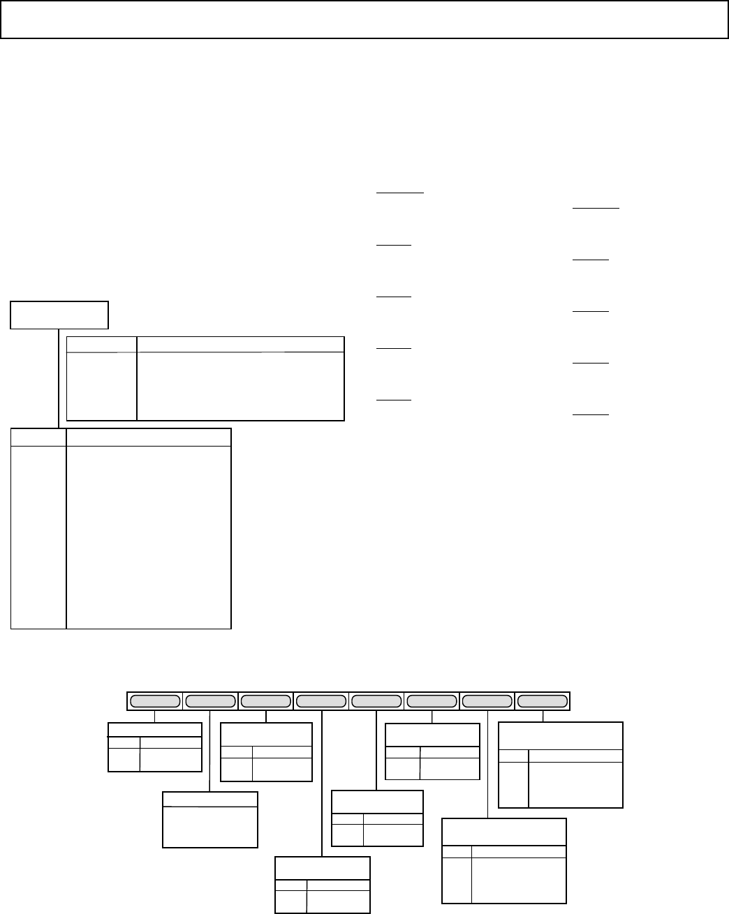
CONTROL REGISTERS
A large bank of registers can be accessed using the Address reg-
ister and C1–C0. Access is made first by writing the Address
Register with the appropriate address to point to the particular
Control Register, and then performing an MPU access to the
Control Register.
ADDRESS REGISTER
(A10–A0)
(A10–A0) REGISTER ACCESS
4FF–412 RESERVED
411 COMMAND REGISTER 2
410 RESERVED
40F RESERVED
40E RESERVED
40D RESERVED
40C RESERVED
40B RESERVED
40A RESERVED
409 RESERVED
408 RESERVED
407 BLUE DAC GAIN ERROR REGISTER
406 GREEN DAC GAIN ERROR REGISTER
405 RED DAC GAIN ERROR REGISTER
004 RESERVED
403 RESERVED
402 RESERVED
401 RESERVED
400 COMMAND REGISTER 1
000–3FF RESERVED
C1 C0 R/W
0 0 0 WRITE TO ADDRESS REGISTER (LOWER BYTE)
0 1 0 WRITE TO ADDRESS REGISTER (UPPER BYTE)
1 0 0 WRITE TO REGISTERS
0 0 1 READ FROM ADDRESS REGISTER (LOWER BYTE)
0 1 1 READ FROM ADDRESS REGISTER (UPPER BYTE)
1 0 1 READ FROM REGISTERS
1 1 X RESERVED
Figure 6. Control Registers
COMMAND REGISTER 1 (CR1)
(Address Register (A10–A0) = 400H)
This register contains a number of control bits as shown in the
diagram. CR1 is an 8-bit wide register.
Figure 7 shows the various operations under the control of CR1.
This register can be read from as well as written to. Bit CR16 is
reserved and should be set to logic “1.”
COMMAND REGISTER 1-BIT DESCRIPTION
BLANK Control on Inverted Outputs (CR10):
This bit specifies whether the video
BLANK is to be decoded
onto the inverted analog outputs or ignored.
SYNC Control on Inverted Outputs (CR11)
This bit specifies whether the video SYNC is to be decoded
onto the inverted analog outputs or ignored.
SYNC Recognition on Blue (CR12)
This bit specifies whether the video SYNC input is to be de-
coded onto the IOB analog output or ignored.
SYNC Recognition on Green (CR13)
This bit specifies whether the video SYNC input is to be de-
coded onto the IOG analog output or ignored.
SYNC Recognition on Red (CR14)
This bit specifies whether the video SYNC input is to be de-
coded onto the IOR analog output or ignored.
Pedestal Enable Control (CR15)
This bit specifies whether a 0 IRE or a 7.5 IRE blanking pedes-
tal is to be generated on the video outputs.
Display Mode Control (CR17)
This bit controls whether the display is interlaced or noninterlaced.
CR17 CR16 CR15 CR14 CR13 CR12 CR11 CR10
CR16 = 0
(RESERVED)
ZERO MUST BE
WRITTEN TO THIS BIT
INTERLACE ENABLE
0 DISABLE
1 ENABLE
CR17
PEDESTAL ENABLE
CONTROL
0 0 IRE
1 7.5 IRE
CR15
SYNC RECOGNITION
CONTROL (IOG)
0 IGNORE
1 DECODE
CR13
SYNC RECOGNITION
CONTROL (IOB)
0 IGNORE
1 DECODE
CR12
SYNC RECOGNITION
CONTROL (IOR)
0 IGNORE
1 DECODE
CR14
PEDESTAL CONTROL
(IOR, IOG, IOB)
0 DISABLE BLANK ON
INVERTED OUTPUTS
1 DECODE BLANK ON
INVERTED OUTPUTS
CR10
SYNC CONTROL
(IOR, IOG, IOB)
0 DISABLE SYNC ON
INVERTED OUTPUTS
1 DECODE SYNC ON
INVERTED OUTPUTS
CR11
Figure 7. Command Register 1
Komentáře k této Příručce