ADV7129
–8–
REV. 0
PIN DESCRIPTION
Mnemonic Function
R7–R0[A . . . H] Red Pixel Port Inputs (TTL Compatible Inputs). Eight sets of eight bits latched on the rising edge of
LOADIN.
G7–G0[A . . . H] Green Pixel Port Inputs (TTL Compatible Inputs). Eight sets of eight bits latched on the rising edge of
LOADIN.
B7–B0[A . . . H] Blue Pixel Port Inputs (TTL Compatible Inputs). Eight sets of eight bits latched on the rising edge of
LOADIN.
BLANK Composite Blank (TTL Compatible Input). This video control signal drives the analog outputs to the blanking
level. When
BLANK is at logic “0,” the pixel inputs are ignored. Pedestal selection is controlled by Bit CR15
of Command Register 1.
BLANK is latched on the rising edge of LOADIN.
ODD/
EVEN Odd/Even Field Input (TTL Compatible Input). This input indicates which field of the frame is being dis-
played. An even field is selected by setting ODD/
EVEN to logical “0.” An odd field is selected by setting
ODD/
EVEN to logical “1.” ODD/EVEN should be changed only during vertical blank.
HSYNC Horizontal-Sync Input (TTL Compatible Input). This control signal is latched on the rising edge of LOADIN.
VSYNC Vertical-Sync Input (TTL Compatible Input). This control signal is latched on the rising edge of LOADIN.
CSYNC Composite-Sync Input (TTL Compatible Input). This video control signal drives the analog outputs to the
SYNC level. It is only asserted during the blanking period and does not override any other control or data in-
put. CR14, CR13 or CR12 of Command Register 1 must be set together with CR11 or Command Register 1 to
decode
SYNC onto the IOR/IOR, IOG/IOG or IOB/IOB analog outputs, otherwise the SYNC input is ignored.
CE Chip Enable Input (TTL Compatible Input). This input must be set to logic “0” when writing or reading over
the data bus (D7–D0). Internally, data is latched on the rising edge of
CE.
R/
W Read/Write pin (TTL Compatible Input). This signal is latched on the falling edge of CE. A high level indi-
cates a read operation and a low level indicates a write operation.
C0, C1 Register select pins (TTL Compatible Inputs). These inputs select which MPU port register is selected for
writing or reading. Data is latched on the falling edge of
CE.
D7–D0 Data Bus (TTL Compatible Input/Output Bus). Data, including color palette values and device control infor-
mation is written to and read from the device over this 8-bit, bidirectional databus. Any unused bits of the
data bus should be terminated through a resistor to either the digital power plane (V
CC
) or GND.
LOADIN Pixel Data Load Input (TTL Compatible Input). This input latches the multiplexed pixel data, including
BLANK, HSYNC, VSYNC, CSYNC, and ODD/EVEN into the device. This rising edge of this signal is used
to latch in the video signal inputs. It is also used as a reference frequency to generate an 8 × multiple pixel
clock using the fixed reference onboard PLL.
LOADOUT Pixel Data Load Output (TTL Compatible Output). This digital output is PCLK/8. If the onboard phase lock
loop is used, it has the same phase as LOADIN.
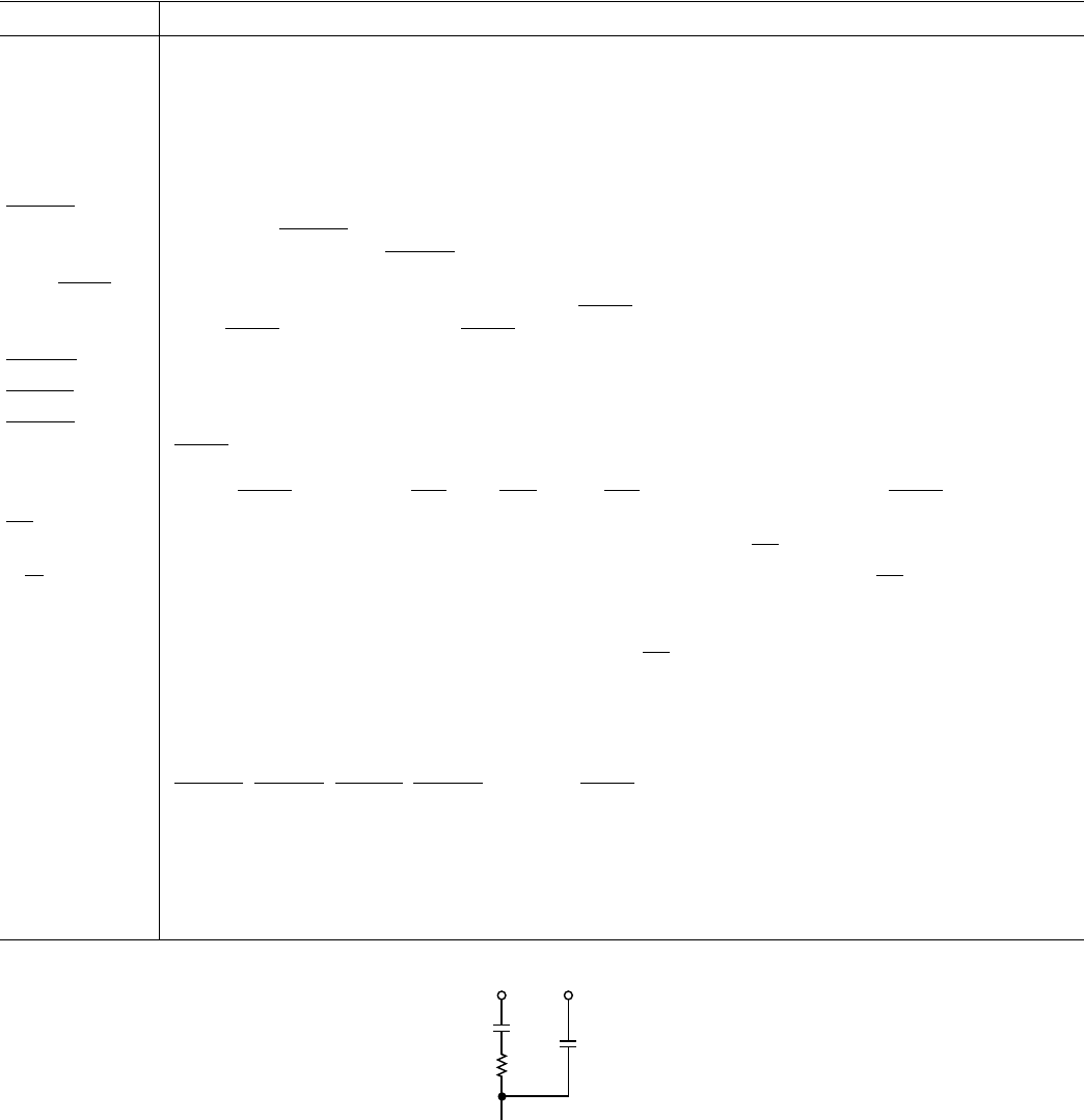
LPF Low-Pass Filter Pin. This pin stabilizes the internal PLL. The following network is recommended.
0.001µF
100Ω
LPF
0.1µF
V
AA
Figure 5.
Komentáře k této Příručce